Why all layers shows on top (in layout) in orcad? Cadence orcad 17.2 full download Orcad schematic
OrCAD Capture 44,000 Schematic Symbols - YouTube
Orcad symbol library available for osd335x c-sip Orcad/allegro libraries Best way to check orcad schematic – use altium designer
Creating schematic symbols using cadence orcad
Orcad social octavosystemsSchematic diagram drawn by orcad software Cis orcadOrcad tutorial for beginners || add net name in schematic.
Orcad capture add part properties in schematic symbols. #orcad #allegro(pdf) creating schematic symbols in orcad capture6.pdf... · creating Orcad circuit example parallel tutorial amplifier pcb completed systems layout simulation headphone pspice prepared shown pictureOrcad tutorial overview.

The easy way to get pcb symbols, footprints & 3d models
Orcad/allegro librariesSymbol orcad create part library capture pins add Orcad walk-through tutorialsDesign schematics in orcad by alfun777.
Orcad capture connector power schematics electrical schematic ground software add circuits simulating resistor components connect few three pages next willLab 3 introduction orcad schematic symbols hardware timer How to edit the symbols at schematic level in orcad pcb designSchematic orcad.
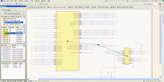
Orcad schematics screen full
Mouser pcb footprint footprints orcadOrcad pcb design tutorial Orcad, placing symbols, schematic capture, pcb cadOrcad schematic symbol.
Orcad, placing symbols, schematic capture, pcb cadHow to master orcad schematic capture: a step-by-step tutorial Allegro orcad pcb 3d model downloaded mapping setup included package select step menu if partOrcad tutorial.

How to create custom schematic symbols
Pcb orcad 17 viewer cadence nuclearrambo wordpressDesign schematics in orcad by alfun777 Orcad capture 44,000 schematic symbolsHow to create a new symbol in orcad.
Orcad schematic portfolioHow to create schematic in orcad(ac to dc converter)#orcad#orcadtool# Orcad setup footprints cis assignOrcad allegro symbol pcb footprints symbols 3d models ensure folder included important downloads must library.

Schematic capture orcad sparkfun credit notes
Schematic orcad capture sparkfun credit notesOrcad schematics screen full How to assign footprints to schematic symbolsOrcad layout layers shows why top stack.
Orcad accurately critical quickly identify components advancedOrcad symbol schematic Orcad sdt schematic viewerCreating schematic symbol in orcad.

Orcad schematics schematic capture libraries existing components getting tutorials techref app
.
.


